- 您现在的位置:买卖IC网 > Sheet目录47 > W83772G (Nuvoton Technology Corporation of America)IC H/W MONITOR 8-TSSOP
W83772G
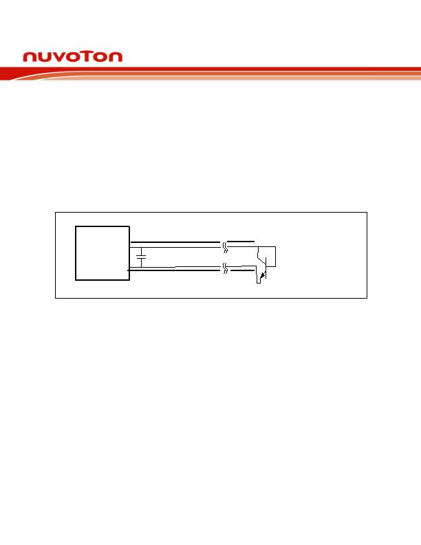
8. PCB LAYOUT GUIDE
Pin 3 & Pin 4 are typically connected to a thermal diode. Here are some recommendations for optimal
operation:
a) Place remote diode as close as possible to W83772G.
b) Route D+ and D- lines away from clock generators, memory buses, or any high frequency buses.
c) Place shield traces, which are connecting to board ground, flanking D+/D- to shield the noise.
d) It is recommended that the bypass capacitor with 2200pF should be placed close to W83772G to
filter the noise from motherboard digital signals.
e) Place a 0.1uF bypass capacitor close to the VCC pin.
The connection diagram is shown as the following.
D+
D-
W83772G
2200pf
GND
GND
Figure 3.
Publication Release Date: May 22, 2006
- 7 -
Version: 1.0
发布紧急采购,3分钟左右您将得到回复。
相关PDF资料
W83L786G
IC H/W MONITOR 28-SSOP
X96011V14IZ
IC SENSOR TEMP BIAS SGL 14-TSSOP
XR4151CP-F
IC CONV VF/FV 8PDIP
XRP7714ILB-0X14-F
IC REG 5OUT BCK/LINEAR 40TQFN
XRP7740ILB-0X18-F
IC REG 5OUT BCK/LINEAR 40TQFN
XRP7740ILBTR-F
IC REG 5OUT BCK/LINEAR 40TQFN
ZDS1009TA
IC CURRENT MIRROR SOT223-8
ZXCT1008FTA
IC CURRENT MONITOR 1% SOT23-3
相关代理商/技术参数
W83773G
制造商:Nuvoton Technology Corp 功能描述:IC H/W MONITOR 8TSSOP
W83775G
制造商:Nuvoton Technology Corp 功能描述:IC H/W MONITOR 8TSSOP
W83777F
制造商:未知厂家 制造商全称:未知厂家 功能描述:Peripheral IC
W83781
制造商:WINBOND 制造商全称:Winbond 功能描述:MONITORING IC
W83781D
制造商:Winbond Electronics Corp 功能描述:SPECIALTY ANALOG CIRCUIT, PQFP48
W83781G
功能描述:IC MONITOR H/W 48-LQFP RoHS:是 类别:集成电路 (IC) >> PMIC - 热管理 系列:- 标准包装:1 系列:- 功能:温度监控系统(传感器) 传感器类型:内部和外部 感应温度:-40°C ~ 125°C,外部传感器 精确度:±2.5°C 本地(最大值),±5°C 远程(最大值) 拓扑:ADC,比较器,寄存器库 输出类型:2 线 SMBus? 输出警报:无 输出风扇:无 电源电压:2.7 V ~ 5.5 V 工作温度:-40°C ~ 125°C 安装类型:表面贴装 封装/外壳:SOT-23-8 供应商设备封装:SOT-23-8 包装:Digi-Reel® 其它名称:296-22675-6
W83782
制造商:WINBOND 制造商全称:Winbond 功能描述:MONITORING IC
W83782D
制造商:WINBOND 制造商全称:Winbond 功能描述:H/W MONITORING IC
